

 产品中心Products
 热线电话:0512-69565898
公司地址:苏州市工业园区青剑湖科技园2A
热线电话:0512-69565898
公司地址:苏州市工业园区青剑湖科技园2A
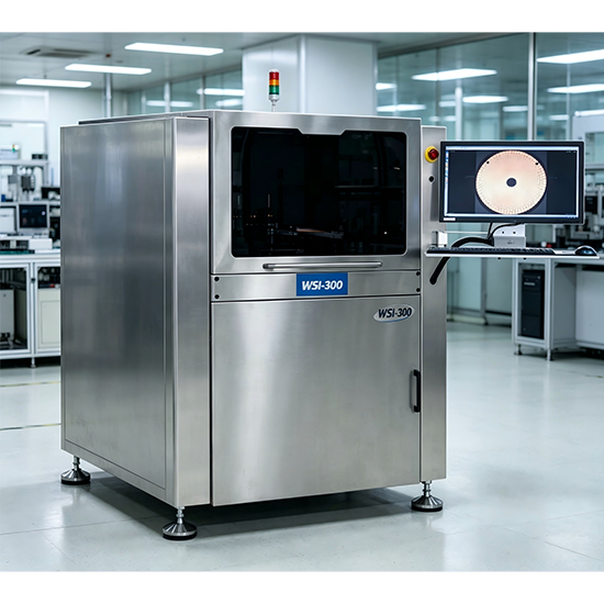
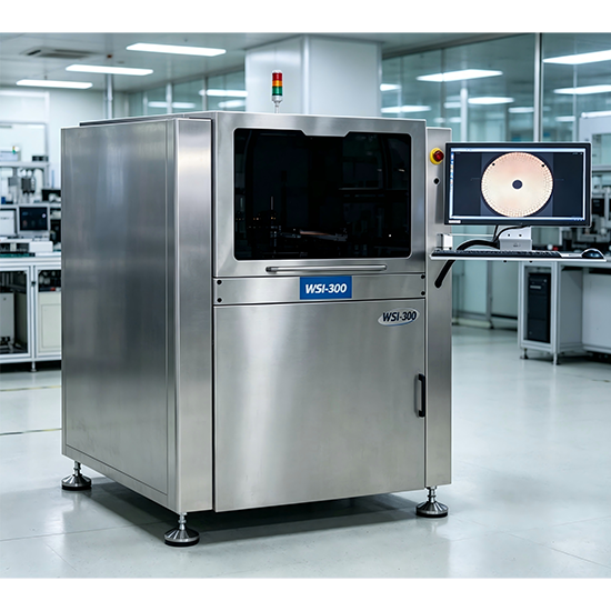
WSI-300 Wafer Printing & Bumping Stencil Inspector is specifically designed for the precision inspection of stencils used in wafer flux printing and solder ball bumping processes.
全国服务热线:0512-69565898
在线咨询
WAFER Flux or ball Drop stencil inspection
WSI-300 Wafer Printing & Bumping Stencil Inspector is specifically designed for the precision inspection of stencils used in wafer flux printing and solder ball bumping processes
Currently, there is a severe lack of effective means for incoming quality control and in-process cleaning validation of wafer-level stencils. Traditional manual inspection is time-consuming and labor-intensive. Given the high cost of 8/12-inch bumping stencils, manual checks can only roughly identify physical damage, while failing to fully inspect critical parameters such as aperture accuracy, thickness, quantity, and quality. A 100% full inspection cannot be achieved, and it is impossible to accurately judge specifications between >40μm and <200μm under high process requirements. Microscopy only allows for partial visual checks, leading to high omission rates. Without data management, problems with expensive bumping and printing stencils cannot be detected in a timely and effective manner. The WSI-300 addresses these gaps by enabling: new stencil aperture accuracy and quality inspection, used stencil cleaning effect verification, foreign object detection, tension measurement, and stencil precision comparison.
Product Features and Benefits
4.11 Incoming Inspection for Flux Printing/Bumping Stencils: Perform comprehensive detection of new stencils before they enter production, ensuring the rationality and correctness of aperture designs.
4.12 In-Process Control & Monitoring of Flux Printing/Bumping Stencils: Track and record changes in stencil precision and tension over different usage periods, ensuring stencil service life and traceable data management. 4.13 Process Data Overlay & Analysis for Flux Printing/Bumping Stencils: Enable stencil process data overlay to optimize manufacturing processes.
SPECIFICATIONS
No. | Description | Specifications |
1 | Wafer Cleaning Stencil Size | Max. L737 × W737 × H40 (mm) |
2 | Stencil Inspection Imaging System | 12 MP camera; optical resolution: 3.45~6.9 μm |
3 | Minimum Detectable Bumping Stencil | Minimum detectable aperture: 40 μm; minimum detectable damage: ≥15 μm |
4 | 3D Stencil Thickness Measurement | Resolution: 0.4 μm; accuracy: ±2 μm |
5 | Automatic Stencil Tension Test | High-precision tension meter with multi-point programmable positions; accuracy: ±1 N/cm; range: 0~50 N |
6 | Automatic Laser Focus & Distance Measurement | Laser-based fast and precise focusing; capable of measuring stencil deformation, etc. |
7 | Barcode Scanning Information Management | Fast recipe and data management via barcode scanning |
8 | Offline Automatic Recipe Design Software | Offline automatic Gerber recipe design software |
9 | Gerber Customization Function | Customizable Gerber definition |
10 | Bottom Illumination | Green coaxial LED light |
11 | Resolution | 3.45~6.9 μm (resolution within the same FOV: 0.345 μm) |
12 | FOV Size | 28.45 mm × 21.2 mm (±0.5 mm) |
13 | Stencil Frame Size | Standard: supports frames up to 813 × 813 × 60 mm |
14 | Maximum Stencil Measuring Range | Standard: 570 × 600 mm |
15 | Machine Dimensions | 1250 × 1340 × 1530 mm |
16 | Machine Weight | 1280 kg |